Intel held a live event yesterday, the newly appointed CEO Pat Gelsinger gave a speech and demonstrated the Xe-HPC high-performance GPU with a 7nm process, code-named Ponte Vecchio.
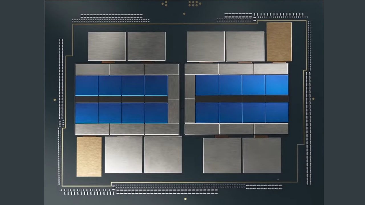
This product encapsulates 47 chips, a total of more than 100 billion transistors, Intel said this is currently one of the largest and most complex processors in the world. Intel’s GPU core uses a 7nm EUV process, but different small chips use different processes.
This product utilizes Intel’s most advanced packaging technology, and it took 2 years from design to implementation. In the live broadcast, Intel showed the real shots of this large GPU processor, the interface on the back, and the engineering board for testing.
Like this? https://t.co/6OVEssFppl pic.twitter.com/dG8nm58hLz
— Raja Koduri (Bali Makaradhwaja) (@RajaXg) March 24, 2021
It can be seen that this product is palm-sized and uses dual-channel water cooling for heat dissipation. It is currently being built on the production line. Intel engineer Raja Koduri previously revealed 7 advanced technologies used in this product:
- Intel 7nm process technology
- TSMC 7nm process technologyIntel Foveros 3D packaging process
- Intel EMIB Embedded Multi-Chip Interconnect Bridge Technology
- 10nm enhanced Super Fin process
- Rambo Cache caching technology
- HBM2 high-speed video memory
- Types of chiplets included in Intel’s Ponte Vecchio processor:
- 16 Xe HPC computing units (internal/external)
- 8 Rambo (internal)
- 2 Xe Base (internal)
- 11 EMIB (internal)
- 2 Xe Link (external)
- 8 HBM (external)
As can be seen from the figure, this processor can be divided into two independent GPU units structurally, each group contains a complete computing module, I/O unit, HBM2 video memory, etc. tipster shared a clearer chip structure.
In general, Intel’s Xe HPC GPU processor with an MCM structure uses the most advanced Foveros 3D packaging technology, which integrates multiple chips from different generation plants and using different processes on a platform, and uses EMIB high-speed connection technology.
For data exchange, each computing unit can use Rambo Cache and HBM2 video memory, providing ample performance release. Not only that, Intel Xe Link technology can interconnect up to six Xe HPC processors to further improve performance.
Intel previously reported that Xe HPC GPUs will have more than 1,000 EUs, and the Xe-LP architecture DG1 that has been leaked so far has a maximum of 96 EUs and 768 stream processors. The highest specifications of Intel Xe HP GPU can reach 2048 EU, 16384 stream processors, 36 TFLOP floating-point operation speed, TDP up to 400W-500W.