2020 will be over in less than two weeks. The end of the year is another season of review and summary. What technological innovations did Intel have this year? Insiders in the chip industry gave a comment, and the 10nm SuperFin process ranked second.
This selection was launched by Twitter user Witeken, who not only frequently broke the latest AMD/Intel information but was also a professional in the chip industry. The selection was mainly at the chip technology level and was very professional.
According to his choice, Intel’s largest technological innovation in 2020 is the Foveros 3D stack on the Lakefield processor. This is a new 3D packaging technology that can encapsulate IP cores of different technologies. The 5 cores of Lakefield are 1. One big and four small, using 10nm and 22nm process respectively.
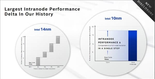
The second innovation is the first 10nm SuperFin process on Tiger Lake. This is also the most important advancement for Intel in CPU technology this year. It uses a brand-new Super MIM device and claims to have achieved the largest performance improvement in a single node, exceeding 15%.
Although many people think that Intel’s 10nm SF process is not as advanced as TSMC’s 7nm and 5nm, but don’t forget that Intel’s foundation in semiconductor technology is still there. There are indeed many innovations in the 10nm process.
The third major innovation is silicon-based optoelectronics. The bandwidth is 6 times that of PCIe 6.0. This is also a key area of Intel’s future semiconductor technology. Optoelectronics technology is also leading, but it has not yet been commercialized on a large scale.
There are three other new technologies, including low-temperature process, A, MX instruction set, and Statix 10 NX FPGA chip, etc., which are more professional than the previous three.

(Source)