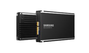
According to the latest report, Samsung Electronics recently set up a new test and packaging (TP) center in the DS (system product) department.
Join tip3x on Telegram
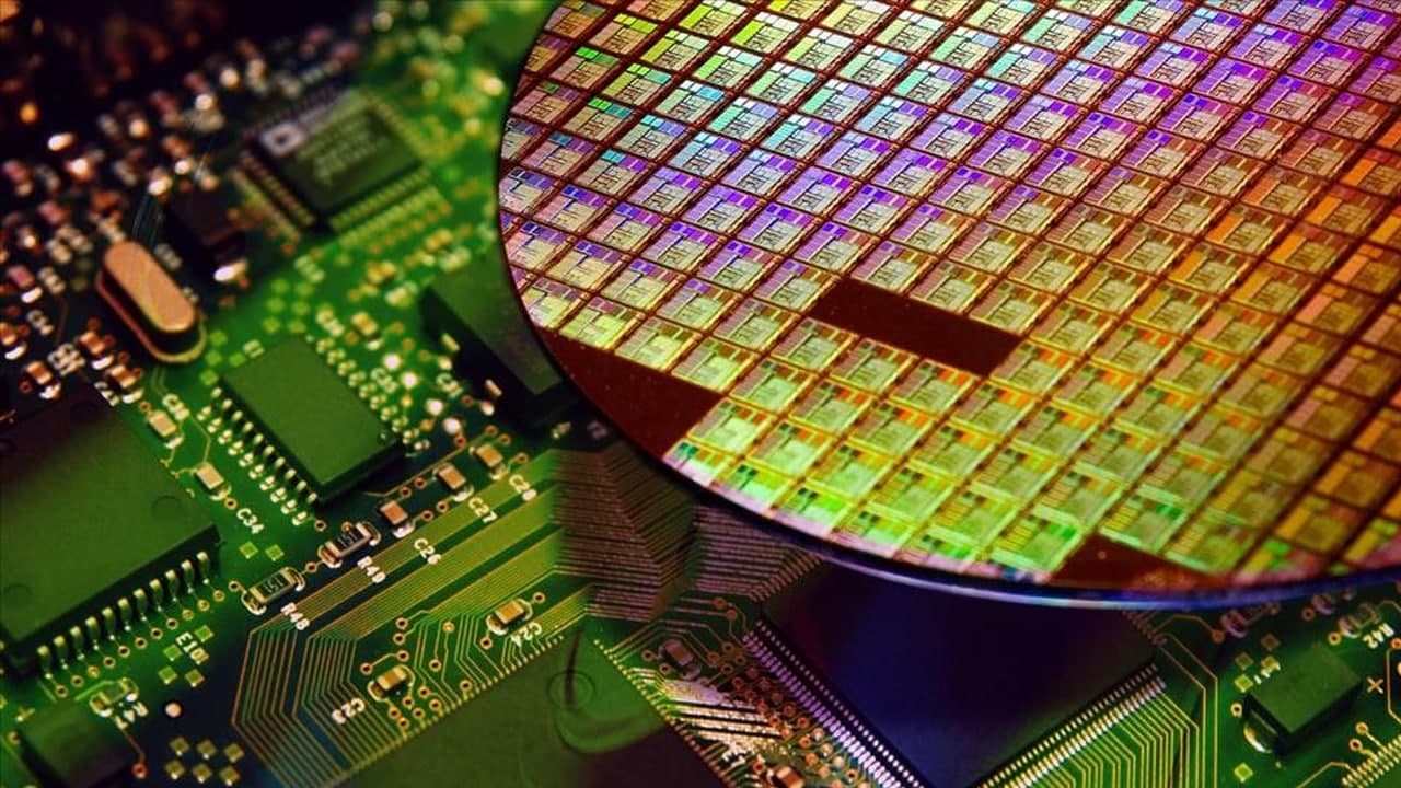
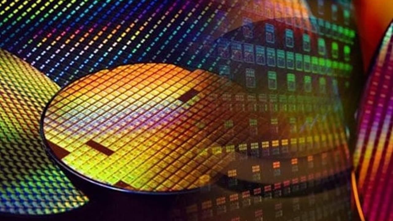
Moreover, the sources believe that Samsung’s move may be a prelude to its expansion of investment in the field of packaging and testing, as advanced packaging has increasingly become the focus of competition among current leading companies, and TSMC and Intel are also investing heavily in this field.
 Furthermore, Samsung Electronics has announced its next-generation 2.5D packaging solution H-Cube concept in November last year and has a certain M&A layout in this field.
According to estimates by the research institute GIA, the global semiconductor advanced packaging market is estimated to be US$36.7 billion in 2022 and is expected to reach US$50.6 billion by 2026, with a compound annual growth rate of 7.7%.